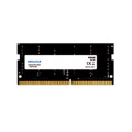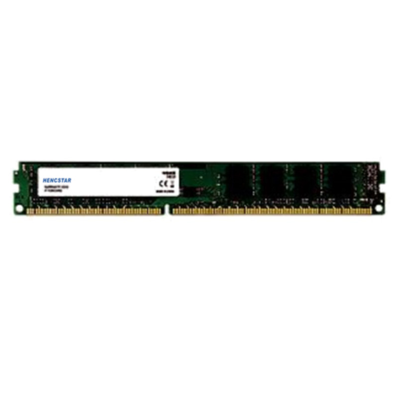
DDR3 UDIMM Memory Module Specifications
Get Latest Price| Payment Type: | L/C,T/T,D/A |
| Incoterm: | FOB,EXW,CIF |
| Transportation: | Ocean,Air,Express,Land |

Shenzhen Hengstar Technology Co., Ltd.
| Payment Type: | L/C,T/T,D/A |
| Incoterm: | FOB,EXW,CIF |
| Transportation: | Ocean,Air,Express,Land |
Model No.: NSO4GU3AB
| Selling Units | : | Piece/Pieces |
4GB 1600MHz 240-Pin DDR3 UDIMM
Revision History
| Revision No. | History | Draft Date | Remark |
| 1.0 | Initial Release | Apr. 2022 |
|
![]()
Ordering Information Table
| Model | Density | Speed | Organization | Component Composition |
| NS04GU3AB | 4GB | 1600MHz | 512Mx64bit | DDR3 256Mx8 *16 |
Description
Hengstar Unbuffered DDR3 SDRAM DIMMs (Unbuffered Double Data Rate Synchronous DRAM Dual In-Line Memory Modules) are low power, high-speed operation memory modules that use DDR3 SDRAM devices. NS04GU3AB is a 512M x 64-bit two rank 4GB DDR3-1600 CL11 1.5V SDRAM Unbuffered DIMM product, based on sixteen 256M x 8-bit FBGA components. The SPD is programmed to JEDEC standard latency DDR3-1600 timing of 11-11-11 at 1.5V. Each 240-pin DIMM uses gold contact fingers. The SDRAM Unbuffered DIMM is intended for use as main memory when installed in systems such as PCs and workstations.
Features
Power Supply: VDD=1.5V (1.425V to 1.575V)
VDDQ = 1.5V (1.425V to 1.575V)
800MHz fCK for 1600Mb/sec/pin
8 independent internal bank
Programmable CAS Latency: 11, 10, 9, 8, 7, 6
Programmable Additive Latency: 0, CL - 2, or CL - 1 clock
8-bit pre-fetch
Burst Length: 8 (Interleave without any limit, sequential with starting address “000” only), 4 with tCCD = 4 which does not allow seamless read or write [either on the fly using A12 or MRS]
Bi-directional Differential Data Strobe
Internal (self) calibration; Internal self calibration through ZQ pin (RZQ: 240 ohm ± 1%)
On Die Termination using ODT pin
Average Refresh Period 7.8us at lower than TCASE 85°C, 3.9us at 85°C < TCASE < 95°C
Asynchronous Reset
Adjustable data-output drive strength
Fly-by topology
PCB : Height 1.18” (30mm)
RoHS Compliant and Halogen-Free
Key Timing Parameters
| MT/s | tRCD(ns) | tRP(ns) | tRC(ns) | CL-tRCD-tRP |
| DDR3-1600 | 13.125 | 13.125 | 48.125 | 2011/11/11 |
Address Table
| Configuration | Refresh count | Row address | Device bank address | Device configuration | Column Address | Module rank address |
| 4GB | 8K | 32K A[14:0] | 8 BA[2:0] | 2Gb (256 Meg x 8) | 1K A[9:0] | 2 S#[1:0] |
Pin Descriptions
| Symbol | Type | Description |
| Ax | Input | Address inputs: Provide the row address for ACTIVE commands, and the column |
| BAx | Input | Bank address inputs: Define the device bank to which an ACTIVE, READ, WRITE, or |
| CKx, | Input | Clock: Differential clock inputs. All control, command, and address input signals are |
| CKEx | Input | Clock enable: Enables (registered HIGH) and disables (registered LOW) internal circuitry |
| DMx | Input | Data mask (x8 devices only): DM is an input mask signal for write data. Input data is |
| ODTx | Input | On-die termination: Enables (registered HIGH) and disables (registered LOW) |
| Par_In | Input | Parity input: Parity bit for Ax, RAS#, CAS#, and WE#. |
| RAS#, | Input | Command inputs: RAS#, CAS#, and WE# (along with S#) define the command being |
| RESET# | Input | Reset: RESET# is an active LOW asychronous input that is connected to each DRAM and |
| Sx# | Input | Chip select: Enables (registered LOW) and disables (registered HIGH) the command |
| SAx | Input | Serial address inputs: Used to configure the temperature sensor/SPD EEPROM address |
| SCL | Input | Serial |
| CBx | I/O | Check bits: Used for system error detection and correction. |
| DQx | I/O | Data input/output: Bidirectional data bus. |
| DQSx, | I/O | Data strobe: Differential data strobes. Output with read data; edge-aligned with read data; |
| SDA | I/O | Serial |
| TDQSx, | Output | Redundant data strobe (x8 devices only): TDQS is enabled/disabled via the LOAD |
| Err_Out# | Output (open | Parity error output: Parity error found on the command and address bus. |
| EVENT# | Output (open | Temperature event: The EVENT# pin is asserted by the temperature sensor when critical |
| VDD | Supply | Power supply: 1.35V (1.283–1.45V) backward-compatible to 1.5V (1.425–1.575V). The |
| VDDSPD | Supply | Temperature sensor/SPD EEPROM power supply: 3.0–3.6V. |
| VREFCA | Supply | Reference voltage: Control, command, and address VDD/2. |
| VREFDQ | Supply | Reference voltage: DQ, DM VDD/2. |
| VSS | Supply | Ground. |
| VTT | Supply | Termination voltage: Used for control, command, and address VDD/2. |
| NC | – | No connect: These pins are not connected on the module. |
| NF | – | No function: These pins are connected within the module, but provide no functionality. |
Notes:The pin description table below is a comprehensive list of all possible pins for all DDR3 modules. All pins listed may not be supported on this module. See Pin Assignments for information specific to this module.
Functional Block Diagram
4GB, 512Mx64 Module (2Rank of x8)


Module Dimensions
Front view

Front view

Notes:
1.All dimensions are in millimeters (inches); MAX/MIN or typical (TYP) where noted.
2.Tolerance on all dimensions ±0.15mm unless otherwise specified.
3.The dimensional diagram is for reference only.


Privacy statement: Your privacy is very important to Us. Our company promises not to disclose your personal information to any external company with out your explicit permission.
Fill in more information so that we can get in touch with you faster
Privacy statement: Your privacy is very important to Us. Our company promises not to disclose your personal information to any external company with out your explicit permission.