


DDR4 UDIMM Memory Module Specifications
Get Latest Price| Payment Type: | L/C,T/T,D/A |
| Incoterm: | FOB,CIF,EXW |
| Transportation: | Ocean,Land,Air,Express |

Shenzhen Hengstar Technology Co., Ltd.
| Payment Type: | L/C,T/T,D/A |
| Incoterm: | FOB,CIF,EXW |
| Transportation: | Ocean,Land,Air,Express |
Model No.: NS08GU4E8
| Selling Units | : | Piece/Pieces |
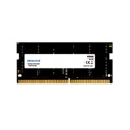
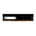
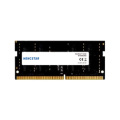
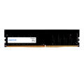
8GB 2666MHz 288-Pin DDR4 UDIMM
Revision History
| Revision No. | History | Draft Date | Remark |
| 1.0 | Initial Release | Apr. 2022 |
|
Ordering Information Table
| Model | Density | Speed | Organization | Component Composition |
| NS08GU4E8 | 8GB | 2666MHz | 1Gx64bit | DDR4 1Gx8 *8 |
Description
Hengstar Unbuffered DDR4 SDRAM DIMMs (Unbuffered Double Data Rate Synchronous DRAM Dual In-Line Memory Modules) are low power, high-speed operation memory modules that use DDR4 SDRAM devices. NS08GU4E8 is a 1G x 64-bit one rank 8GB DDR4-2666 CL19 1.2V SDRAM Unbuffered DIMM product, based on eight 1G x 8-bit FBGA components. The SPD is programmed to JEDEC standard latency DDR4-2666 timing of 19-19-19 at 1.2V. Each 288-pin DIMM uses gold contact fingers. The SDRAM Unbuffered DIMM is intended for use as main memory when installed in systems such as PCs and workstations.
Features
Power Supply: VDD=1.2V (1.14V to 1.26V)
VDDQ = 1.2V (1.14V to 1.26V)
VPP - 2.5V (2.375V to 2.75V)
VDDSPD=2.25V to 3.6V
Nominal and dynamic on-die termination (ODT) for data, strobe, and mask signals
Low-power auto self refresh (LPASR)
Data bus inversion (DBI) for data bus
On-die VREFDQ generation and calibration
On-board I2C serial presence-detect (SPD) EEPROM
16 internal banks; 4 groups of 4 banks each
Fixed burst chop (BC) of 4 and burst length (BL) of 8 via the mode register set (MRS)
Selectable BC4 or BL8 on-the-fly (OTF)
Databus write cyclic redundancy check (CRC)
Temperature controlled refresh (TCR)
Command/Address (CA) parity
Per DRAM Addressability is supported
8 bit pre-fetch
Fly-by topology
Command/Address latency (CAL)
Terminated control command and address bus
PCB: Height 1.23” (31.25mm)
Gold edge contacts
RoHS Compliant and Halogen-Free
Key Timing Parameters
| MT/s | tCK | CAS Latency | tRCD | tRP | tRAS | tRC | CL-tRCD-tRP |
| DDR4-2666 | 0.75 | 19 | 14.25 | 14.25 | 32 | 46.25 | 19-19-19 |
Address Table
| Configuration | Number of | Bank Group | Bank | Row Address | Column | Page size |
| 8GB(1Rx8) | 4 | BG0-BG1 | BA0-BA1 | A0-A15 | A0-A9 | 1 KB |
Functional Block Diagram
8GB, 1Gx64 Module (1Rank of x8)

Absolute Maximum Ratings
Absolute Maximum DC Ratings
| Symbol | Parameter | Rating | Units | NOTE |
| VDD | Voltage on VDD pin relative to VSS | -0.3 ~ 1.5 | V | 1,3 |
| VDDQ | Voltage on VDDQ pin relative to VSS | -0.3 ~ 1.5 | V | 1,3 |
| VPP | Voltage on VPP pin relative to VSS | -0.3 ~ 3.0 | V | 4 |
| VIN, VOUT | Voltage on any pin except VREFCA relative to VSS | -0.3 ~ 1.5 | V | 1,3,5 |
| TSTG | Storage Temperature | -55 to +100 | °C | 1,2 |
DRAM Component Operating Temperature Range
| Symbol | Parameter | Rating | Units | Notes |
| TOPER | Normal Operating Temperature Range | 0 to 85 | °C | 1,2 |
| Extended Temperature Range | 85 to 95 | °C | 1,3 |
AC & DC Operating Conditions
Recommended DC Operating Conditions
| Symbol | Parameter | Rating | Unit | NOTE | ||
| Min. | Typ. | Max. | ||||
| VDD | Supply Voltage | 1.14 | 1.2 | 1.26 | V | 1,2,3 |
| VDDQ | Supply Voltage for Output | 1.14 | 1.2 | 1.26 | V | |
| VPP | Supply Voltage for DRAM Activating | 2.375 | 2.5 | 2.75 | V | 3 |
Module Dimensions
Front view

Back view


Privacy statement: Your privacy is very important to Us. Our company promises not to disclose your personal information to any external company with out your explicit permission.
Fill in more information so that we can get in touch with you faster
Privacy statement: Your privacy is very important to Us. Our company promises not to disclose your personal information to any external company with out your explicit permission.